


層數 Multilayer Borad Thichness | 1~36 Layer |
板厚 Borad Thichness | 0.2-3.2mm |
高密度互聯 High Density Interconnection | 1+n+1,1+1+n+1+1,2+n+2 |
主要板材 Primary Material Suppliermm | Shengyi﹠EMC﹠ITEQ |
環保產品 Environmental Products | 多層及HDI(ROHS ,halogen- free無鹵素) |
最小線寬間距 line width space | 3/3mil |
最大銅厚 Max Copper foil thickness | 單層2oz |
機械鑽孔 min via hole size | Min:0.2mm |
激光鑽孔 min blind hole size | Min:0.1mm |
半金屬化孔最小孔徑 Minimum semi-metallized hole | Min:0.45mm |
盲埋孔 buried hole | 4-16 layer |
最大生產尺寸 Max production borad size | 520mmX620mm |
電鍍縱橫比 Max Aspect ratio | 8:01 |
線寬間距 line width space | ±10% |
電鍍孔孔徑 Pth Aperture size | ±3mil |
能力 Capability | 通常Current Status |
非電鍍孔孔徑 NPth Aperture size | ±2mil |
孔位精度 hole location Accuracy | ±3mil |
孔中心到孔中心距離 Distance from the center of the hole to the center of the hole | ±4mil |
孔到邊精度 Hole to Edge Precision | ±3mil |
層與層對位精度 layer to layer registertion | ±4mil |
外形公差 Shape Size tolerance | ±4mil |
阻抗公差 Impedance tolerances | ±10% |
最小防焊橋 Min.Solder Mask Dam Width | 绿色油墨:3mil 杂色油墨:4.5mil |
防焊對準度 S/M Registration | ±1.5mil |
最小SMT/QFP焊盤中心距 Min.SMT/QFP Pitch | 10mil |
最小BGA焊盤中心距 Min.BGA Pitch | 12mil |
最大測試點數 Max.Test Points/Board(Universal ET) | 针床测试:16000 |
V-cut深度 | ±4mil |
V-cut角度 | 20°、30°、45° |
V-cut精度 v-cut precision | ±4mil |

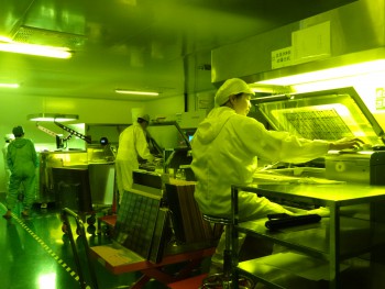
Solder resist exposure

Solder resist
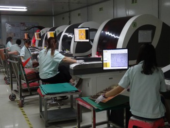
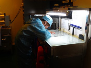
AOI
etching
Map electricity
line
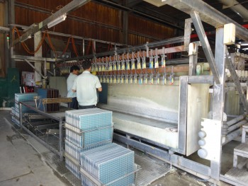
Copper precipitation
drill hole
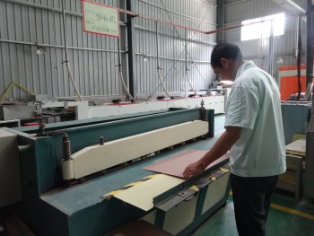
Cutting line
Film test

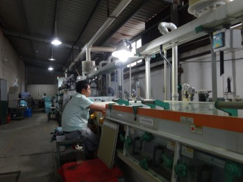
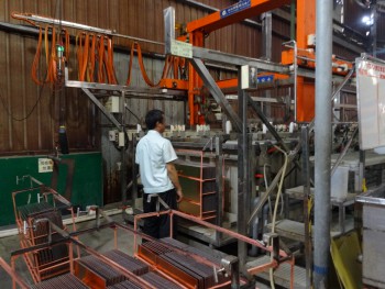
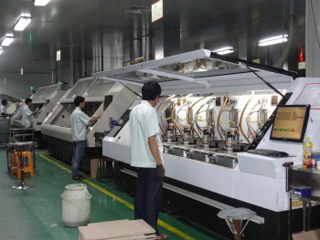
Automatic production line

Factory office building